
With the rapid development of semiconductor technology and the arrival of 5g era, all kinds of modern products are developing in the direction of high voltage, high current, high power and high frequency; the demand for small volume, low energy consumption and high efficiency product appearance is also increasingly strong. As an indispensable part of switching power supply, PC power supply, server power supply, adapter, photovoltaic inverter, UPS, lighting power supply, OBC, charging pile and other products, packaging products with smaller volume and higher efficiency of power semiconductor devices have been unanimously desired. The compact surface mount package (dfn8 * 8) has been launched by Mapson semiconductor in time to meet the needs of the times, which has attracted the attention of many application customers.
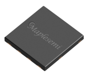
At present, the mainstream of high-power SMT shapes are TO-252 (DPAK), to-263 (d2-pak), dfn5 * 6 and so on. However, due to the limitation of package size and package capacity, the existing packages for the new generation of high-efficiency and small volume products are difficult to meet the demand, so dfn8 * 8 shape package emerges as the times require. Now let's understand the characteristics of dfn8 * 8 shape.
Mapson semiconductor dfn8 * 8 package product launched (Figure 1)
1、 Dfn8 * 8 package features:
Surface mount package
The package height is only 1 mm
■ creepage distance increased to 2.75mm
No pin design
■ enlarged base Island
Excellent thermal performance, similar to to to-263 (d-2pak)
Small size, convenient fit
2、 Package size comparison:
Dfn8 * 8 has more advantages and characteristics than traditional TO-252 and to-263 package sizes
1. The package size of TO-252 is 6.6 * 10 * 2.3 (mm);
The package size of to-263 is 10.2 * 15.15 * 4.7 (mm);
Dfn8 * 8 package size is 8 * 8 * 1.0 (mm), with smaller volume proportion in pasting.
2. The area of TO-252, to-263 and dfn8 * 8 are 66mm2, 154mm2 and 64mm2 respectively.
The area of DFN is more than 50% less than that of to-263.
3. The back fin areas of TO-252, to-263 and dfn8 * 8 are about 23mm ~ 2, 47mm ~ 2 and 34mm ~ 2, respectively.
Dfn8 * 8 back heat sink area is about 50% more than TO-252.
4. The height of TO-252, to-263 and dfn8 * 8 are 2.3mm, 4.7MM and 1mm, respectively
The height is less than TO-252 and to-263.
3、 Compared with traditional plug-in encapsulation:
Compared with the traditional TO-220, TO-247 and to-3pn packages, the SMD package greatly reduces the package size and optimizes the volume and space ratio. Dfn8 * 8 has lower parasitic inductance than TO-252 and to-263 due to its pinless design. The main cooling path is to pass the bare metal pad to PCB to improve the heat dissipation capacity of the package.
N the enlarged base island design can meet the requirements of plug-in power devices in package;
N excellent thermal conductivity, similar to to to-263 (d-2pak), directly adheres to PCB for heat dissipation;
N small volume design can greatly reduce the product space occupation;
N SiC diode, MOSFET (super junction, SiC MOSFET) synchronous packaging market, to meet the needs of more industries;
N excellent RDSON and vfsd are directly applied to more demanding projects;
4、 Practical project display:
Faster, smaller and more efficient is the direction of our engineers. In the fast-paced life of the new era, fast, efficient and convenient application experience has always been favored.
Established in 2014, Mapson semiconductor is located in Shekou, Nanshan District, Shenzhen, which is known as the forefront of China's reform and innovation. It is a complete industrial chain company integrating R & D, design, production, sales and service, and a national high-tech enterprise.
Main power MOSFET (power MOS), trench MOSFET (low voltage MOS), super junction MOSFET (super junction MOS), SiC MOSFET (silicon carbide MOS), SiC diode (silicon carbide diode) and other products.
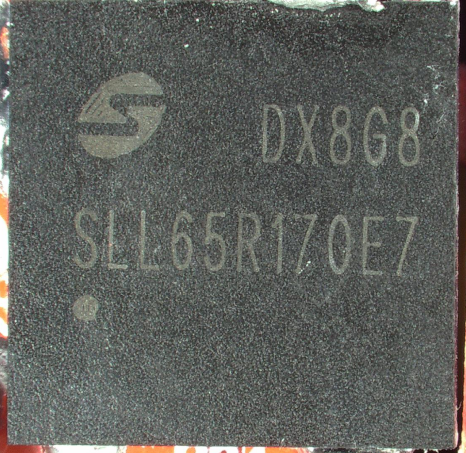
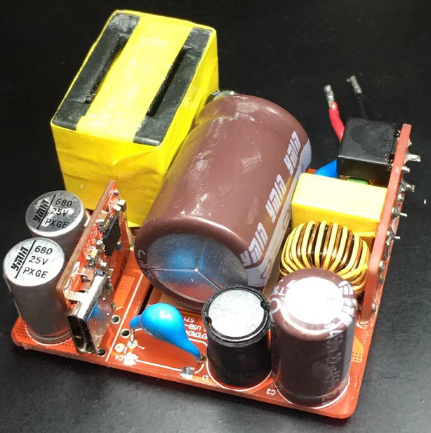
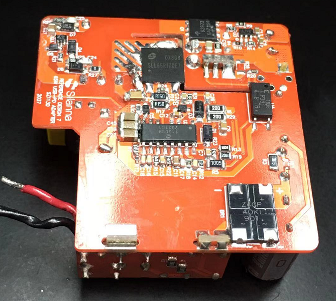
The new dfn8 * 8 superjunction MOSFET of Mapson semiconductor has been in full swing since it was launched into the market. Here is an example of the application of Mapson products (sll65r170e7) in the PD fast charging industry.
Application topology
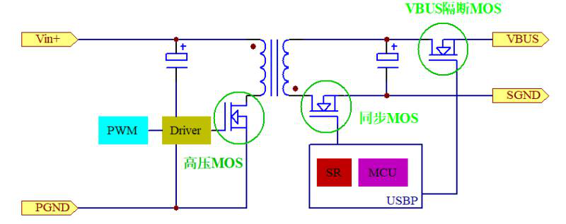
Maple semiconductor dfn8 * 8 package product launch (Figure 2) Mapson semiconductor dfn8 * 8 package product launch (Figure 3)
Fair
■ Datasheet

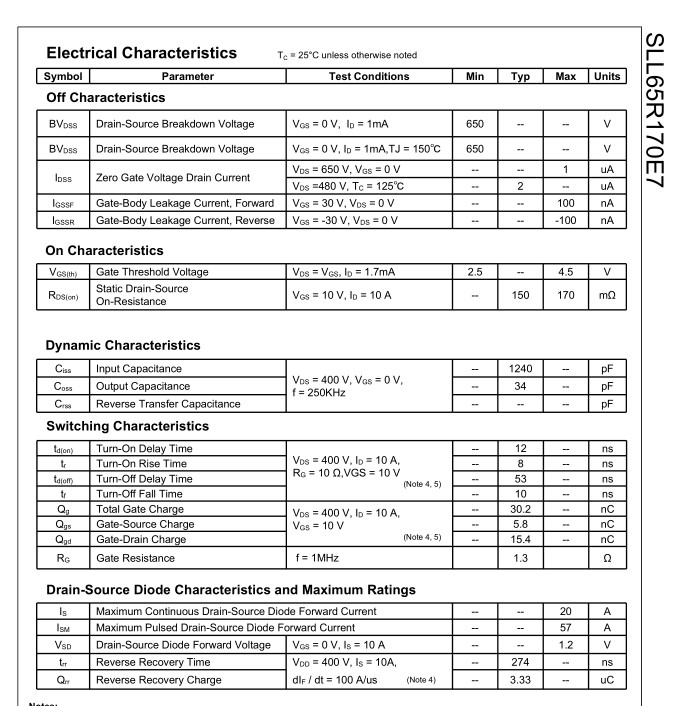
Conclusion
At present, the products of mcpson semiconductor SiC MOSFET and sj-mosfet with dfn8 * 8 package appearance have been on the market at the same time; to meet customer needs, solve customer problems, and provide customers with better service experience has always been the persistent pursuit of every mepson person.
The company focuses on the design, development, testing and sales of power device products based on advanced planar VDMOS, trench MOS, sjmos, SiC SBD, SiC MOS and other process structures. Aiming at consumer electronics, industry and new energy, we are committed to becoming a world-class power component company.
The company has many years of experience in the power industry FAE engineers, packaging engineers and many sales personnel with strong business ability. We are not only committed to providing high-quality semiconductor products for customers, but also pay more attention to providing high-quality after-sales service. In order to meet the needs of customers, the company can help customers to complete the R & D plan, design drawing board, product selection, product testing and final products to meet all the needs of customers.
In this increasingly competitive market, mepson semiconductor adheres to the business philosophy of "innovation, pragmatism, efficiency and win-win" to provide you with the most suitable semiconductor solutions and is your best strategic partner. In the ever-changing market, we continue to move forward, we have everything you need, more and more detailed product information are welcome to consult.
